Fig. 5 presents the overall circuit diagram. The proposed
sub-BGR consists of a bandgap core circuit, comparison block, analog MUX, and stacked self-cascode
MOSFET (SCM). The bandgap core circuit generates all
voltages required for segmented curvature compensation.
The comparison block performs temperature segmentation
and transfers the information of segmented temperature
range to an analog MUX. With the information,
the MUX outputs segment-wise corrected CTAT voltage,
$V_{CTAT,lin}$, by multiplexing voltages in the bandgap core.
Finally, the stacked SCM generates reference voltage by
adding a PTAT voltage to the $V_{CTAT,lin}$. The details of circuit
implementation will be discussed in this section.
Overall circuit diagram of the proposed BGR.
1. Bandgap Core Circuit
The bandgap core circuit produces temperaturedependent
voltages, $V_{C,1}$ and $V_{P,1-P,8}$ for temperature
segmentation and $V_{C,1-C,8}$ for segment-wise correction.
The $V_{C,1}$ is the voltage copied from $V_{EB1}$ by amplifier A1.
Since the voltage difference between $V_{C,1}$ and $V_{EB2}$ is applied
to $R_C$, the bias current, $I_{BIAS}$, can be expressed as
follows:
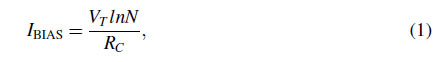
where $V_T = kT/q$ is the thermal voltage exhibiting PTAT,
N is the area ratio of $Q_2$ and $Q_1$, and is set to 8, considering
both common centroid layout and size.With a current mirror
$M_{P3}$ and a resistor string $R_{P,1-8}, V_{P,1-P,8}$ are expressed
as
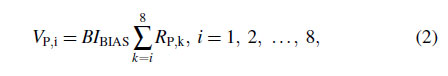
where B is theW=L ratio of the pMOS current mirror from
$M_{P1} (orM_{P2})$ to $M_{P3}$ and is set to 8, considering the tradeoff
between power consumption and the size of the $R_2$.
The $V_{C,1-C,8}$ utilized to segment-wise correction are generated
by tapping voltages from the RC. $V_{C,1-C,8}$ can be
expressed as
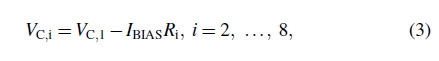
where $R_i$ is the divided resistance between the points
where $V_{C,1}$ and $V_{C,i}$ are tapped. The $I_{BIAS}R_i$ in Eq. (3) becomes
the correction voltages mentioned in Section III.
2. Comparison Block and Analog MUX
Fig. 5 also illustrates the comparison block and analog
MUX. $V_{C,1}$ and $V_{P,1-P,8}$, generated from the bandgap core,
are compared using comparators. As the $V_{C,1}$ intersects
with $V_{P,1-P,8}$, creating temperature cross points, the comparator
outputs, $D_{1-8}$, can provide the information about
the segmented temperature range divided by these points.
The $D_{1-8}$ is decoded to one-hot code, SEL<1:9>, which
is used for the analog MUX to outputVC;i at corresponding
segment, resulting $V_{CTAT,lin}$.
For the low power consumption, the proposed sub-BGR
uses the large resistance of $R_C$ and $R_{P,i}$. However, the
use of large resistance induces significant thermal noise
to comparator input. This may cause the comparator output
to change abruptly near the temperature cross points
which degrades the TC. Therefore, a hysteresis comparator
which is utilized in [
8,
9] is applied in the proposed
BGR to ensure stable operation through hysteresis characteristic.
3. Stacked SCM
The stacked SCM is applied [
10] for linear TC compensation.
The SCM structure composed of $M_t$ and $M_b$ is
presented in Fig. 5. The SCM produces $V_{rmSCM}$, which exhibits
PTAT characteristic dependent on the ratio of both
the bias current and device size. The $V_{rmSCM}$ is expressed
as
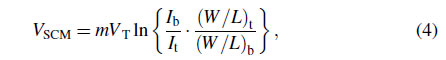
where m is the subthreshold slope factor, I and W=L are
the bias current and aspect ratio, respectively. Moreover,
in the stacked SCM, four $V_{rmSCM}$s are stacked to achieve
higher TC, whose absolute value is the same as TC of
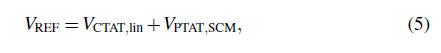
$V_{CTAT,lin}$, but with the opposite sign. Finally, the stacked PTAT voltage, $V_{PTAT,SCM}$, is added to the $V_{CTAT,lin}$ using a
unity gain buffer, $A_2$, resulting $V_{REF}$. The $V_{REF}$ can be expressed
as
and TC of $V_{REF}$ becomes
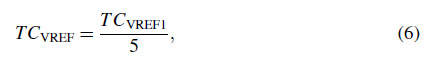
where $TC_{VREF}$ is TC of $V_{REF}$ and $TC_{VREF1}$ is TC of $V_{REF1}$
which is the reference voltage without curvature compensation,
as shown in Fig. 4(a). Since $V_{REF1}$ is divided into
nine segments symmetrically arranged around the middle
segment, $TC_{VREF}$ becomes five times lower than $TC_{VREF1}$.