As shown in Fig. 5, the proposed temperature sensor consists of three main parts: a sensing frontend, a readout circuit, and a digital controller. The sensing frontend employs BJTs to generate ${V}_{\rm BE0}$ and ${V}_{\rm BE1}$. These signals are
processed by the readout circuit, utilizing the 1-bit second-order incremental delta-sigma analog-to-digital converter ($\Delta \Sigma$ ADC) to produce digital values for temperature reading. The digital controller provides control signals and clocks required for overall operation.
To achieve the accuracy requirements of the temperature sensor with only a single PTAT trimming at room temperature (RT), error sources that contribute to non-PTAT errors should be mitigated [3]. Therefore, errors caused by device mismatches and finite $\beta$ should be mitigated to make the PTAT error due to process spread in ${V}_{\rm BE}$ the dominant error source [15].
1. Sensing Frontend
$\textbf{1) Circuit overview:}$ Fig. 6 shows the circuit diagram of the sensing frontend, which consists of the biasing circuit and the bipolar core. The PTAT bias current is generated by the feedback loop which includes an error amplifier, current sources, polysilicon resistors, and PNP transistors. The biasing circuit forces the difference between $V_{\rm BE}$s ($\Delta$$V_{\rm BE}$) of the $Q_{\rm BIAS0}$ and $Q_{\rm BIAS1}$ across the resistors ($R_{\rm BIAS0}$ or $R_{\rm BIAS1}$) to generate a PTAT\textit{ I}${}_{\rm BIAS}$. The generated current is mirrored through the current sources to bias $Q_{0}$ and $Q_{1}$, generating $V_{\rm BE0}$ and $V_{\rm BE1}$ in the bipolar core [
3].
Circuit diagram of the sensing frontend.
$\textbf{2) Error reduction design techniques:}$ If $\beta$ is sufficiently large such that $\beta /(\beta+1)$ effectively equals 1, the influence of $\beta$ spread in Eqs. (1) and (2) can be neglected. However, in the process used, the $\beta$ of the PNP transistor is approximately 3.5, causing $V_{\rm BE}$ to exhibit a non-PTAT error resulting from the $\beta$ spread [16]. Therefore, a $\beta$-compensation technique is employed to generate the $I_{\rm BIAS}$ proportional to $(\beta+1)/\beta$ [16]. Assume that the $\beta$ of all four PNP transistors are the same. The $I_{\rm BIAS}$ with the $\beta$-compensation technique can be expressed as
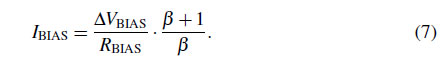
Substituting $I_{\rm BIAS}$ from Eqs. (7) into (1) and (2) yields
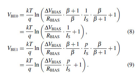
This technique makes the $V_{\rm BE}$s of the $Q_{0}$ and $Q_{1}$ independent of $\beta$ by canceling out $\beta/(\beta+1)$ in Eqs. (1) and (2). The accuracy of the $\beta$-compensation technique can be degraded by the $\beta$ mismatch of the four PNP transistors ($Q_{\rm BIAS0}$, $Q_{\rm BIAS1}$, $Q_{0}$, and $Q_{1}$) [17]. To mitigate the mismatch of the $\beta$ without quantization noise folding, bitstream-controlled DEM is employed [11,15]. However, at high temperatures, $I_{\rm S}$, which is proportional to the emitter area, increases exponentially with temperature [12], resulting in significant nonlinearity in both $V_{\rm BE}$ and $\Delta$$V_{\rm BE}$ [10]. Therefore, the PNP transistors in the sensing frontend are designed with consideration for matching requirements and the impact of $I_{\rm S}$ at high temperatures.
$\textbf{3) Implementation:}$ The biasing circuit and the bipolar core each use a pair of 2 $\mu$m $\times$ 2 $\mu$m PNP transistors: $Q_{\rm BIAS0}$ and $Q_{\rm BIAS1}$, and $Q_{0}$ and $Q_{1}$, respectively. Total 12 unit current sources are employed to bias the $Q_{\rm BIAS0}$, $Q_{\rm BIAS1}$ pair and the $Q_{0}$, $Q_{1}$ pair at the 1:5 ratio with DEM switches to average the unit bias current $I_{\rm BIAS}$. The $I_{\rm BIAS}$ value is set to 300 nA (at $27^\circ$C) with $R_{\rm BIAS0} = R_{\rm BIAS1} = 175$ k$\Omega$, considering the power consumption and the settling requirement of the sampling capacitor in the readout circuit. A conventional folded-cascode topology with a dc gain of over 84 dB across the operating temperature range is used for the error amplifier ${A}_{\rm E}$ in the biasing circuit. As the offset and $1/{f}$ noise of the ${A}_{\rm E}$ cause non-PTAT errors, chopping is employed to mitigate them [11].
$\beta$-compensation technique is implemented by adding resistors ${R}_{\beta0}$ ($= R_{\rm BIAS0}/5$) and ${R}_{\beta1}$ ($= R_{\rm BIAS1}/5$) in series with the bases of $Q_{\rm BIAS0}$ and $Q_{\rm BIAS1}$ in the biasing circuit, respectively. To enable swapping between $Q_{\rm BIAS0}$ and $Q_{\rm BIAS1}$ in the biasing circuit, the $R_{\rm BIAS0}$, ${\mathrm{R}}_{\beta0}$ pair and the $R_{\rm BIAS1}$, ${R}_{\beta1}$ pair are connected, respectively. Similarly, in the bipolar core, DEM logic swaps $Q_{0}$ and $Q_{1}$ by exchanging the current ratio.
2. Readout Circuit
$\textbf{1) Architecture:}$ At high temperatures, the leakage current of the sampling switches increases. Fig. 7 shows the simplified sampling network and associated leakage paths. $I_{leak1}$ is caused by reverse diodes in the on-state switch, while $I_{leak2}$ and $I_{leak3}$ are due to the off resistance of the off-state switches [
13]. These leakages not only distort the bias current in the bipolar core transistors but also introduce errors in the charge sampled onto the sampling capacitors. Since both on-state and off-state switches induce leakage paths, these effects are proportional to the total number of switches in the sampling network [
12,
13]. Unlike the two architectures presented in [
3] and [
18], this paper employs a readout circuit with only two differential sampling capacitors, as in [
13]. This approach significantly reduces the total number of required switches to six, compared to the zoom ADC architecture in [
18], which relies on hundreds of sampling and DEM switches. Consequently, both the reduced number of sampling switches and the absence of DEM switches in the capacitor array mitigate the impact of switch leakage currents in the sampling network at high temperatures.
Simplified sampling network and associated leakage paths.
A required ADC resolution to achieve a temperature sensing resolution of less than $0.025^\circ$C can be calculated by the following equation [10]:
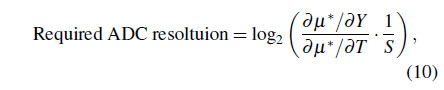
where the ${S}$ is target sensing resolution, ${Y}$ ($= 4 \cdot \Delta V_{\rm BE}/V_{\rm BE1}$) is the digitized ratio, and $\mu^{*}$ is the linear PTAT output. Based on the simulation results, the required ADC resolution is determined to be 15.5-bit.
Circuit diagram of the readout circuit.
$\textbf{2) Charge-Balancing:}$ Figs. 8 and 9 illustrate a circuit diagram of the readout circuit and its simplified timing diagram. Detailed charge-balancing process for digitizing the ${Y} = 4 \cdot \Delta V_{\rm BE}/V_{\rm BE1}$ is as follows: At each $\Phi_{\Delta \Sigma }$ period, the first integrator samples either $V_{\rm BE0}$ or $\Delta V_{\rm BE}$ during four clock phases $\Phi_{1}$ and $\Phi_{2}$, with the total sampled charge varying depending on the ${bs}$. When ${bs} = 0$, $\Delta V_{\rm BE}$ is sampled four times, integrating a charge proportional to $4 \cdot \Delta V_{\rm BE}$. While, when ${bs} = 1$, $\Delta V_{\rm BE}$ is sampled three times and $- V_{\rm BE0}$ is sampled once, resulting in a charge proportional to $3 \cdot \Delta V_{\rm BE} - V_{\rm BE0}$. Due to the ADC's feedback, the average integrated charge is zero, and with the average of ${bs}$ defined as ${Y}$, this charge-balancing scheme satisfies the following equation [3]:
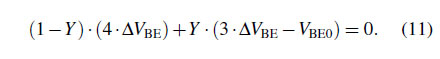
As $3 \cdot \Delta V_{\rm BE} - V_{\rm BE0}$ is equivalent to $4 \cdot \Delta V_{\rm BE} - V_{\rm BE1}$, Eq. (11) can be calculated as shown in the following equations [19]:
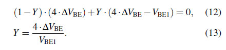
As a result, through Eqs. (11) to (13), this scheme generates the previously mentioned ratio ${Y}$.
$\textbf{3) Implementation:}$ The circuit diagram of the readout circuit is illustrated in Fig. 8. Only two differential sampling capacitors are employed to sample $V_{\rm BE0}$, $V_{\rm BE1}$, and $\textit{gnd}$ using six sampling switches. Additionally, to reduce leakage current in the off-state, the switches connected to $\textit{gnd}$ are implemented using high-threshold voltage devices. The size of the C${}_{S1}$ is set to 2.5 pF, considering the ${kT}/{C}$ noise, while C${}_{S2}$, C${}_{A}$, and C${}_{FF}$ are set to 200 fF, given the relaxed conditions due to noise shaping [16,20]. $A_{1}$ and $A_{2}$ employ folded-cascode OTAs, providing a dc gain of over 97 dB across the operating temperature range. Correlated-double sampling is used to reduce offset and $1/{f}$ noise of the first integrator [21]. System-level low-frequency chopping (CHL) is further applied to address residual offset [19]. The CHL is implemented digitally, eliminating the need for additional switches.
Timing diagram of the readout circuit.
Simplified timing diagram is shown in Fig. 9. The first integrator operates with non-overlapping clocks, $\Phi_{1}$ and $\Phi_{2}$, while the second integrator and the switched capacitor adder operate at half the frequency of the first integrator, using duty-cycle-adjusted non-overlapping clocks, $\Phi_{3}$ and $\Phi_{4}$. The first integrator samples outputs of the sensing frontend ($V_{\rm BE0}$ and $V_{\rm BE1}$) or $\textit{gnd}$ during four clock phases $\Phi_{1}$ and $\Phi_{2}$, based on the value of ${bs}$. During the fourth phase, the first integrator's output is sampled onto $C_{\rm S2}$ of the second integrator during $\Phi_{4}$ phase and subsequently integrated during the following $\Phi_{3}$ phase. The ${bs}$ is generated by the single-bit quantizer with $\Phi_{\Delta \Sigma}$. Oversampling ratio (OSR) of 512 is employed to achieve the required ADC resolution [22].